Tool to be used in Reactive Ion Etching (RIE), a major process for semiconductor nanofabrication, primarily in R&D organizations\
Bangalore based Hind High Vacuum Co. Pvt. Ltd. (HHV), announced that it has developed a versatile R&D tool for the semiconductor industry. Entirely designed and developed at the Bangalore facility of HHV, this tool would be used in Reactive Ion Etching (RIE), a major process for semiconductor nanofabrication.
RIE combines both physical sputtering and the chemical activity of the 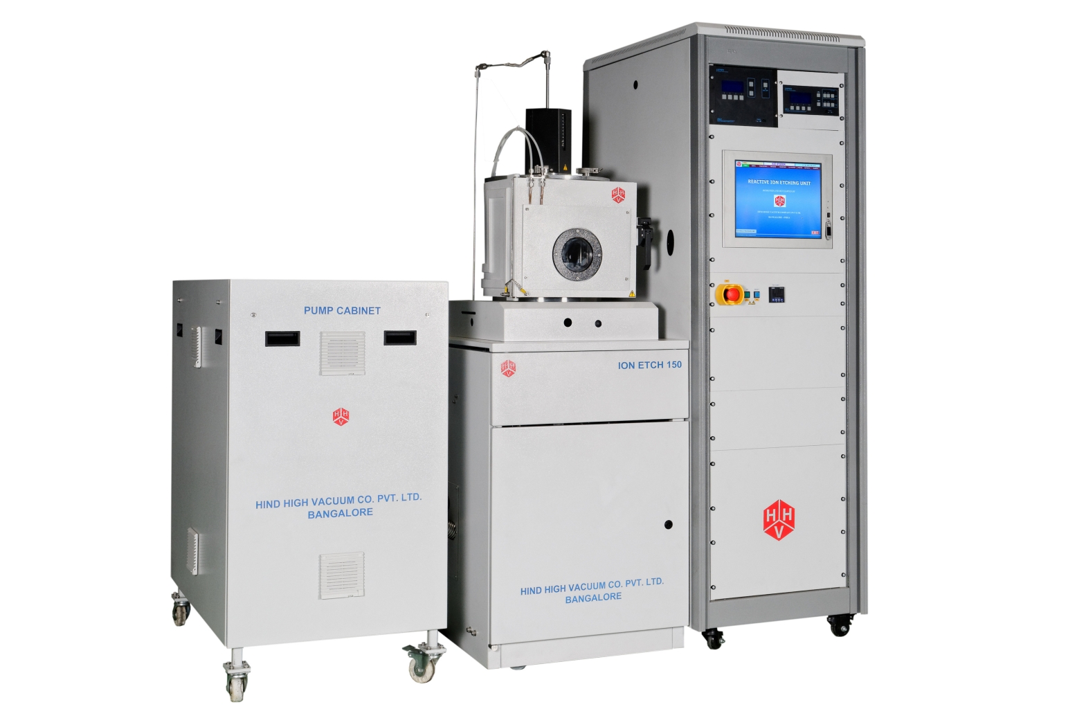 reacting species to ensure high etches anisotropy as well as greater material selectivity. It is the processes of choice for transferring well defined patterns from masks to the substrate to manufacture semiconductor devices and integrated circuits due to its cleanliness, superior etch anisotropy, improved uniformity control and enhanced etch selectivity.
“RIE process is popularly used for machining and etching the materials for high performance nano and micro scale devices, fabrication of integrated circuits (ICs), MEMS and NEMS based sensors and devices” said Mr Prasanth Sakhamuri, Managing Director, HHV. “We are proud to have indigenously developed such a sophisticated and versatile RIE tool, targeted at R&D centres catering to the semiconductor industry, at an affordable price with assured quality and repeatability”.
The system is completely automated and is PC controlled. An associated dynamic oxidation abatement system facilitates neutralization of the processed gases before it is exhausted to the atmosphere.
For specific applications, this RIE tool can also be used as a sputter etching system (non-reactive etching) or as a chemical etching system (non-plasma based etching) as well.