Unique cluster type thin film deposition system, successfully installed at customer site, a leading nuclear research centre in India
 Bangalore based Hind High Vacuum Co. Pvt. Ltd. (HHV), announced that it has developed a unique thin film technology solution for the nuclear energy sector. Entirely designed and engineered out of its Bangalore facility, this cluster type thin film deposition system has been successfully installed at customer site, a leading nuclear research centre in India.
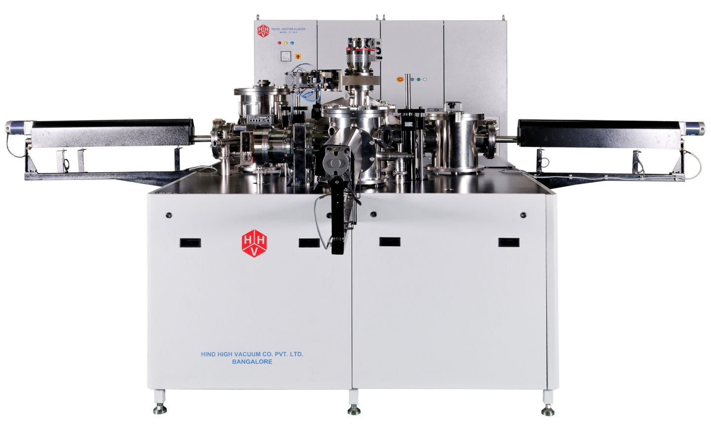
This thin film deposition system is used to deposit a stack of multi-layer thin film coatings to fabricate miniaturised, solid state boron carbide sensors with superior performance and finds incredible applications in the nuclear energy field. It has been successfully demonstrated for functional performance, product quality and repeatability to the most stringent parameters as was laid down by the customer.
Established in 1965 at Bangalore as a specialised enterprise to develop Indian self-reliance in high vacuum technology, HHV has now grown into a multi-location, multi-product group of companies involved in the design, development and manufacture of off-the-shelf and customized equipment and products in the fields of Vacuum Technology, Solar Photovoltaic and Thin Films Technology
“HHV has been committed to serving the scientific and industrial community in optics and thin films with its five decades of expertise in engineering and thin film deposition process development” said Mr Prasanth Sakhamuri, Managing Director, HHV. “The development of this unique cluster type, multi-purpose, versatile, thin film deposition tool with plasma-enhanced chemical vapour deposition (PECVD), sputtering process chambers and a specially designed sublimation system, is yet another demonstration of our unparalleled in-house technological capabilities.”
This cluster type thin film deposition tool has 2 PECVD process chambers to fabricate p-n junction layers, 1 sputtering process chamber to sputter various magnetic and non-magnetic metal films, 1 substrate loading /unloading chamber, 1 transfer chamber and 2 sublimation units to feed the precursors to the PECVD process chambers.
The cluster type thin film deposition system has been integrated with industrial PC based, PLC and SCADA software for total automation of process and vacuum cycle. An optical emission spectrometer integrated with the PECVD process chambers enables to measure the plasma emission and boron (or) carbon content in the coated boron carbide films.
For the past five decades, HHV has been executing challenging assignments involving thin film techniques to fulfill the needs of Space, Defence, Electronics, Horology and other sectors. Its R&D team has been closely associating with world renowned scientists in thin film technology to develop advanced optical coatings and equipment in this field.