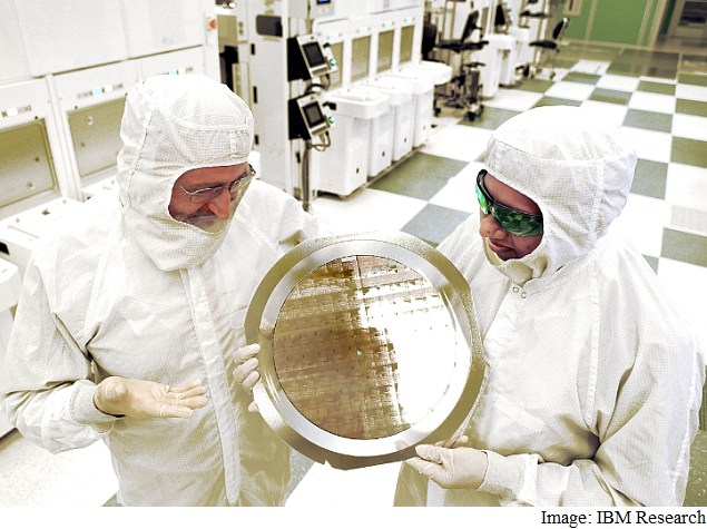
IBM has unveiled the world’s first 7nm microprocessor with working transistors, crossing the 10nm barrier in chip design and reaffirming Moore’s Law.
Made with Common Platform Alliance partners Samsung and GlobalFoundries (whichgot IBM’s chip-making business earlier this year), the 7nm FinFET logic chip design is still in the research phase, and IBM says it will take at least two years to reach commercial production. The estimate shows IBM looks set to leapfrog the cycle, withIntel introducing its first 14nm chips only last year, and its 10nm Cannonlake chips not expected until 2016, at the earliest. Intel has not said anything concrete about its 7nm plans, while TSMC has shared plans to start production on 7nm chips in 2017.
IBM says it has been working on the 7-nanometre transistor fabrication technology for the past five years. It also points to significant jumps in the power-performance ratio, where the new chip can provide comparable performance with greater power efficiency, or greater performance with comparable efficiency. While its 10nm designs improved the ratio by 40-50 percent over 14nm chips, the new 7nm chips push that ratio to 50 percent over 10nm chips.
With 10nm chip designs capable of fitting twice the number of transistors as a 14nm chip, 7nm chips can feature quadruple the number. IBM says with the current working 7nm design it would be possible to fit 20 billion transistors in a microprocessor.
IBM says the advances the firm and its allies made to create the smaller, faster chips on the 7nm node include the channel material, as well as the method to etch transistors into the silicon wafer – known as lithography. Switching away from the traditional silicon, IBM used silicon-germanium alloy (SiGe) for its channel transistors to improve electron mobility, allowing them to switch on and off faster.
The company also becomes the first to use the EUV (extreme ultraviolet) photolithography technique to produce a commercially viable design. The technique, which has been looked at to help make sub-10nm chip designs, utilises ultraviolet light with a wavelength of 13.5nm compared to traditional 193nm wavelength of an argon-fluoride laser. Of course, to etch circuits just 7nm wide, the team claims it had to use special masks in conjunction to etch patterns at that scale.
Several industry watchers say it is more than probable IBM has not yet resolved all the problems involved with EUV lithography, and probably hopes to resolve them by 2017. IBM adds it will be much more difficult to advance beyond the 7nm scale, with carbon nanotubes and gallium-arsenide the proposed materials for the jump – the company had tested its first 9nm transistors with carbon nanotube technology back in 2012.
Source-NDTV